Postdoc - Materials Science
Arizona State University - 1990
Moon Kim
Louis Beecherl Jr. Distinguished Professor
Professor - Materials Science & Engineering
Professional Preparation
Ph.D. - Materials Science
Arizona State University - 1988
Arizona State University - 1988
M.S. - Materials Science
Arizona State University - 1986
Arizona State University - 1986
B.S. - Materials Science
Arizona State University - 1984
Arizona State University - 1984
Research Areas
Research Interests
- Heterogeneous materials integration by wafer bonding
- Fabrication and characterization of various functional nanostructures for applications in nano-electronics, power electronics, energy, electrochemical and bio-devices, and neuromorphic and quantum computing
- Atomic scale characterization of low dimensional nanomaterials
- In-situ TEM study of electrochemical and biological systems
- Nanopore-based sequencing of biomolecules
- Fabrication of 3D nanostructures for nano-robots
- 3D visualization technologies such as virtual reality (VR), image recognition, and hologram for enhanced education
Publications
“Dislocation driven spiral and non-spiral growth in layered chalcogenides: morphology, mechanism, and mitigation,” Y.Nie, A. Barton, R. Addou, Y. Zheng, L. Walsh, S. Eichfeld, R. Yue, C. Comier, C. Zhang, Q. Wang, C. Liang, J. Robinson, M.J. Kim, W. Vanderberghe, L. Colombo, P. Cha, R.M. Wallace, C. Hinkle and K.J. Cho, Nanoscale 10, 15023-15034 (2018) - journal article
“Engineering high-k/SiGe interface with ALD oxide for selective GeOx reduction,” M. Kavrik, P. Ercius, J. Cheung, K. Tang, Q. Wang, B. Fruhberger, M.J. Kim, Y. Taur, P.C. Mclntyre and A.C. Kummel, ACS Appl. Mater. Inter. 11, 15111-15121 (2019). 2019 - journal article
“Engineering the Pd-WSe2 interface chemistry for field effect transistors with high-performance hole contacts”, C. Smyth, L. Walsh, P. Bolshakov-Barrrett, M. Catalano, R. Addou, L. Wang, S. McDonnell, J. Kim, M.J. Kim, C.D. Young, C.L. Hinkle and R.M. Wallace, ACS Appl. Nano. Mater. 2, 75-88 (2019). 2019 - journal article
“Monolithic Integration of Transition Metal Oxide Multiple Quantum Wells on Silicon (001),” J. Ortmann, S. Kwon, A. Posadas, M.J. Kim, and A. Demkov, J. Appl. Phys. 125, 155302 (2019). 2019 - journal article
“Deformation behavior of nanocrystalline and ultrafine-grained CoCr CuFe Ni high-entropy alloys,” S. Nam, J. Hwang, J. Jeon, J. Park, M.J. Kim, D. Bae, J. Kim and H.J. Choi, J. Mater. Res. 34, 720-731 (2019). 2019 - journal article
“Interfacial structure evolution and thermal conductivity of Cu-Zr/diamond composites prepared by gas pressure infiltration,” L. Wang, J. Li, G. Bai, N. Li, X. Wang, H. Zhang, J. Wang, and M.J. Kim, J. Alloys Comp. 781, 800-809 (2019). 2019 - journal article
“Engineering high-k/SiGe interface with ALD oxide for selective GeOx reduction,” M. Kavrik, P. Ercius, J. Cheung, K. Tang, Q. Wang, B. Fruhberger, M.J. Kim, Y. Taur, P.C. Mclntyre and A.C. Kummel, ACS Appl. Mater. Inter. 11, 15111-15121 (2019). 2019 - journal article
“Stiffness measurement of nanosized liposomes using solid-state nanopore sensor with automated recapturing platform,” J.S. Lee, J. Saharia, Y.M. Nuwan, D.Y. Bandera, B. Karawdeniya, G. Goyal, A. Darvish, Q. Wang, M.J. Kim and M. Kim, Electrophoresis 40, 1337-1344 (2019). – featured on the cover 2019 - journal article
Awards
Outstanding Researcher Award - UT-Dallas, School of Engineering [2017]
President’s International Fellow - Chinese Academy of Sciences [2015]
Invited Professor - General Research Institute for Nonferrous Metals [2015]
WCU Visiting Professor - Gwangju Institute of Science and Technology [2012]
Appointments
Louis Beecherl, Jr., Distinguished Professor
UT-Dallas [2014–Present]
Engineering
UT-Dallas [2014–Present]
Engineering
Professor
UT-Dallas [2013–Present]
Arts and Humanities
UT-Dallas [2013–Present]
Arts and Humanities
Fellow
Microscopy Society of America [2012–Present]
Microscopy Society of America [2012–Present]
Director
Industry University Cooperative Research Center [2009–2019]
Industry University Cooperative Research Center [2009–2019]
Professor
UT-Dallas [2008–Present]
Engineering
UT-Dallas [2008–Present]
Engineering
Adjunct Professor
UTSW Medical Center [2007–Present]
Simmons Comprehensive Cancer Center
UTSW Medical Center [2007–Present]
Simmons Comprehensive Cancer Center
Professor
University of Texas at Dallas [2005–Present]
University of Texas at Dallas [2005–Present]
Director
University of Texas at Dallas [2004–Present]
Nano-characterization Facility
University of Texas at Dallas [2004–Present]
Nano-characterization Facility
Associate Professor
University of Texas at Dallas [2003–2005]
University of Texas at Dallas [2003–2005]
Director
University of North Texas [2002–2004]
Facility for Electron Microscopy
University of North Texas [2002–2004]
Facility for Electron Microscopy
Additional Information
Member, Materials Research Society (MRS), Microscopy Society of America (MSA)
News Articles
Jonsson School Engineers Help Develop Tiny Transistor in Novel Way
 In the quest for faster and more powerful computers and consumer electronics, big advances come in small packages.
 The high-performance, silicon-based transistors that control today’s electronic devices have been getting smaller and smaller, allowing those devices to perform faster while consuming less power.
But even silicon has its limits, so researchers at The University of Texas at Dallas and elsewhere are looking for better-performing alternatives.
Scientists Discovery Could Have Powerful Effect on Electronics
 The field of quantum mechanics deals with materials at atomic dimensions, and big discoveries often happen at a very small scale. Researchers in the Erik Jonsson School of Engineering and Computer Science, in collaboration with an international team of engineers and scientists, have uncovered a phenomenon that could have major implications for the development of nano-electronic circuits and devices.
In a recent article published in Nature Communications, the researchers describe for the first time how grown and stacked, atomically thin materials can exhibit a unique transport effect, called negative differential resistance, or NDR, at room temperature.
Activities
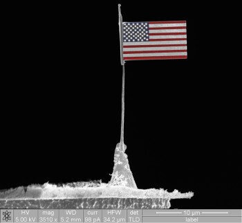
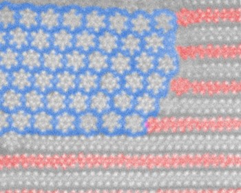
Nano Art Exhibition
Nano Art is a new discipline that discovers and accentuates the artistic beauty of nanometer sized natural and artificial structures. Nano Art can be characterized as one of two means. The first is discovering the artistic value in the images of nanostructures directly observed in the scientific laboratory. The second is the use of natural and artificial materials to create micrometer or even smaller sized sculptures or figures. An instrument such as electron/ion microscope and scanning probe microscope is used to obtain magnified images of such small nanostructures. The recorded images are either presented as is or processed to accentuate its artistic value. Any modification made in the image is disclosed fully.- “Nano Art Exhibit,” UT-D Natural Science and Engineering Research Laboratory (October 26, 2016).
- “Nano Art Exhibit,” UT-Dallas, Davidson-Gundy Alumni Center (January 24, 2018)
Expertise and extensive experience in electron microscopy
- Expertise in high resolution analytical electron microscopy includes HREM phase contrast and STEM Z-contrast imaging, Convergent Beam Electron Diffraction (CBED), energy dispersive x-ray (EDX, electron energy loss spectroscopy (EELS), and in-situ TEM/STEM.
- Served as a lab instructor and a committee member of User Program of the National Facility for HREM at ASU for more than 10 years during his tenure at Arizona State University, conducted extensive interdisciplinary collaborative research involving state-of-the-art TEM nano-characterization.
Development and/or refinement of Research Tools
- Designed and built an ultra high vacuum (UHV) wafer bonding unit to integrate dissimilar materials suitable for electronic and optical properties measurements, fracture mechanical testing, and structural characterization by electron microscopy. There are only two other similar instruments in the world: at Lawrence Livermore National Laboratory and the University of Tokyo Dr. Kim's unit is the one capable of synthesizing planar interfaces (for metals, ceramics and semiconductors) suitable for both microscopy and quantitative interface strength measurements with both control of interface orientation and additional element chemistry.
Professional activity
- Strategic partnerships:
- Nanofactory Instruments AB, Sweden: Recruited to open its U.S. headquarter in Richardson. Established a strategic partnership for the development of new instruments (e.g., in-situ STM-TEM, AFM-TEM and TEM-nanoindentation tools) and collaborative research.
- Japan Electro-Optics Lab (JEOL), Inc. - UTD as its U.S. Southwest Demo Center.
- Protochips, Inc. – Established a strategic partnership for the development of new instruments (e.g., in-situ heating and liquid cell stages) and collaborative research
- Directed the NSF initiated Silicon Wafer Engineering and Defect Science (SiWEDS) Center. Its industry and academic members are: SRC, MEMC, Samsung, Hynix, Siltronic, UTD, NCSU, UoW, Stanford, MIT, Waseda Univ., ASU.
- Served as a reviewer for the following journals: Metallurgical Transactions, Ultramicroscopy, Journal of Electronic Materials, Journal of Applied Physics, Sensors and Actuators, Journal of Materials Science, International Journal of Nanoscience, Microelectronic Engineering, Composite Science and Engineering, Thin Solid Films, ACS Nano, Acta Materialia, Energy and Fuels, Microscopy and Microanalysis, IEEE Transactions on Nanoelectronics, IEEE Electron Device Letters, Environmental Science and Technology, Journal of The Electrochemical Society, and Journal of Nanoengineering and Nanosystems.
- Gave over 130 invited lectures and seminars at National/International conferences, Universities and Research Institutes.
- Taught annually at the internationally renowned ASU Winter School for HREM(2002-2009).
Service to the community
- K-12 outreach program (Provided hands-on experience by visiting RISD elementary schools with lab equipment - "Men in Nano" theme).
- Played a key role in establishing the memorandum of understanding (MOU) for student exchange and collaborative research programs between UTD and other institutions (Korea Institute of Science and Technology (KIST), Korea Advanced Nano Center (KANC), University of Seoul (UOS), Choongnam Technology Park (CTP))
- Established new Nano-Characterization Facility and managed its operation